Quantum memories are fundamental devices in quantum information science as they act as interfaces between the photons, used as information carriers, and atoms, exploited for information storage and processing. The storage of quantum states of light has important applications, for the distribution of quantum information over long distances, e.g. in quantum repeaters, or the synchronization of independent and probabilistic processes, for multiphoton generation. To be useful in quantum information protocols, the quantum memories must fulfill specific requirements, including: on-demand read-out, high efficiency and fidelity, long storage time, and multimodality.
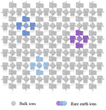
Sketch of an insulating crystal doped with rare earth ions of the same species. The inhomogeneities in the crystal structure affect the RE3+ hosted in different sites by shifting the resonance frequencies, represented by the different colors. S
Rare earth (RE) doped crystals are particularly attractive because they are ensembles of ions naturally trapped in inert media, which thus do not require external trapping fields and ultra-high vacuum chambers. The very narrow homogeneous linewidth associated with a large static inhomogeneous broadening of the crystal field transitions are fundamental resources in view of tailoring, by optical pumping, the specific structures which allow the storage of light pulses. The RE3+ ions can be easily optically addressed, and their coherence properties can be controlled by means of RF fields. As they exhibit transitions both in the optical and in the microwave range, they have the potential to serve not only as photonic memories, but also as microwave memories or interfaces between optical and microwave frequencies, thus opening the way to hybrid systems employing superconducting qubits. As all quantum memories based on atomic ensembles, the RE3+ doped crystals also offer quantum information multiplexing.
With the RE3+ doped materials, we are particularly interested in the development of new telecom-compatible platforms for integrating quantum devices on-chip, with the aim of achieving improved performances due to light confinement over distances exceeding those permitted by the diffraction limit. Moreover, the integration facilitates the scalability and realization of complex optical circuitries in a compact fashion, allegedly less affected by losses and mechanical instability. For example, it would enable the coupling with both on-chip entangled photon sources and superconducting nanowires single photon counters.
The challenges that we address are:
- The engineering of novel materials for improved solid-state quantum devices
A complete understanding of the mechanisms affecting the optical and spin coherence can lead to the development of new materials whose properties can literally be engineered for specific quantum photonics applications. In addition, sophisticated techniques, making use of static or dynamic magnetic field or spin-echo sequences, can be also implemented to push the coherence properties of the materials under investigation up to the limits imposed by the optical and spin state lifetimes.
- The exploration of confined environment for integrated quantum devices
The general trend in quantum photonics is to move towards integrated systems. In this framework, we want to extend the investigation of the rare earth ions in confined structures, as e.g. waveguides, nano-composite materials, nano-photonics structures. This research line includes both fundamental aspects, as the analysis of the effect of the light confinement on the optical and spin-coherence or on the phononic population, and the implementation of protocols for non-linear interactions between photons mediated by the strong light-atom interaction.
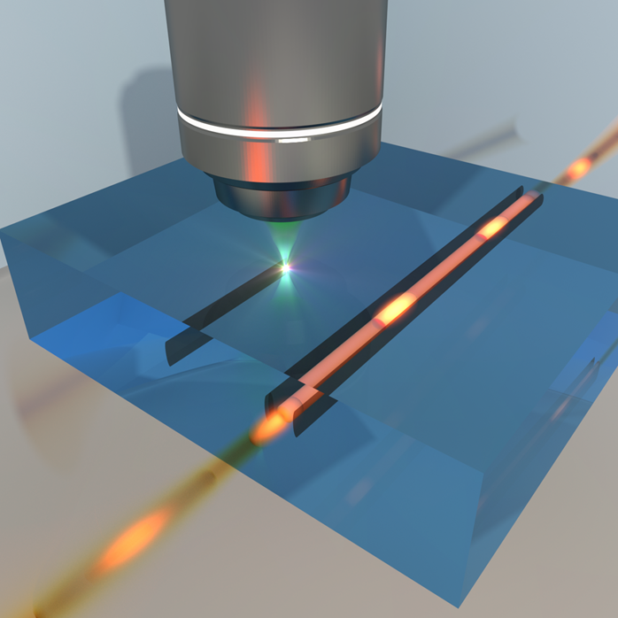
Example of the waveguide inscription in a transparent material doped with RE3+ ions by means of femtosecond laser irradiation. Credit: FAST Group @IFN-CNR