 Transition metal dichalcogenides (TMDs) are atomically thin materials which offer a crucial feature lacking in graphene: a bandgap. These two-dimensional semiconductors ‘beyond graphene’ can produce a remarkably wide range of electronic and optical properties. Beyond merely replacing conventional materials such as Si or GaAs in conventional electronic or photonic devices, these 2D materials can also have unique physical properties such as spin-valley physics that are being actively explored for ‘valleytronics’ and coherent quantum bits based on the valley pseudo-spin. Further, stacking the individual layers of different 2D crystals leads to heterostructures which are not limited by lattice mismatch between adjacent layers as is the case in conventional semiconductors. This opens unlimited possibilities to engineer optoelectronic materials with specific properties. Recently, localized excitons in TMDs have been shown to emit non-classical light yet appear to maintain the general electronic and magneto-optical characteristics (e.g., direct band gap, large Coulomb interaction energy, and large exciton g-factor) of the host 2D semiconductor. We aim to realize a new quantum photonic platform based on this system.
In particular, we are addressing the following topics and questions:
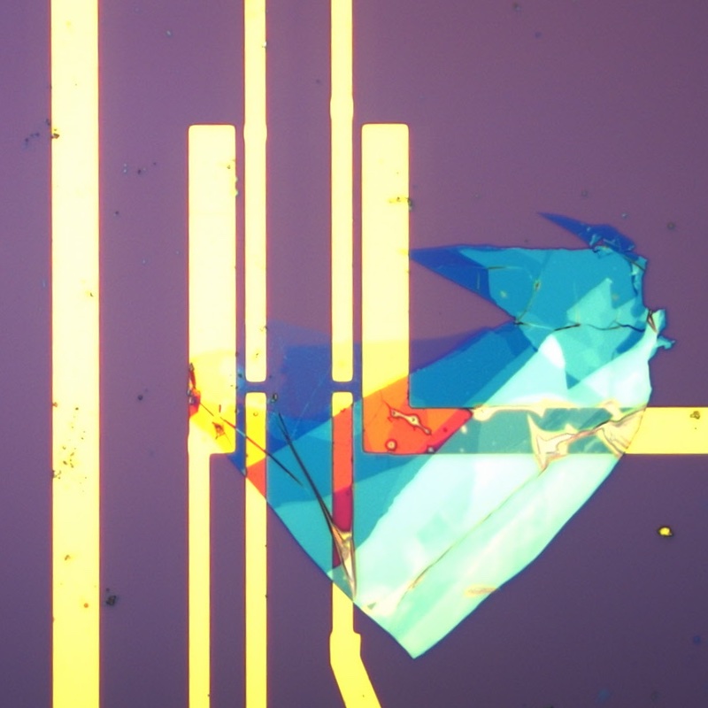
- An essential challenge is to identify the precise origin of the localized excitons, which is still under debate. A complimentary challenge is to try to induce or create artificial quantum dots in pristine 2D materials using external perturbations, e.g. electronic confinement created by local strain, tunable electronic gates, or Coulomb engineering via a structured dielectric environment.
- Incorporating 2D materials with quantum emitters into fully functional electronic devices, with a particular goal of observing Coulomb blockade to enable deterministic loading of electrons one-by-one into the quantum emitter and unlock the exploration of spins and valleys in the system. Additionally, encapsulating the active 2D material could provide much needed emitter stability.
- Coherent light-matter interaction: can we coherently manipulate spins and excitons in this material platform? How coherent and indistinguishable can the single photons be? Is there a way to entangle spins and photons in the 2D quantum emitters?
- Due to their 2D nature, the quantum emitters can be incorporated into hybrid photonic structures for efficient light-matter interaction and integrated photonics. How close to perfect extraction of single photons can we achieve? Can emitters be deterministically incorporated into scalable photonic chips based on materials with a strong electro-optic effect?
- Huge strains, up to ∼11%, can be induced in atomically thin materials. To what degree can strain-tuning (local or global) be used to engineer the electronic, spin-valley coupling, and optical properties?