The goal of this research line is to create quantum opto-electronic devices for secure quantum networking and quantum sensing using silicon carbide, a semiconductor of wide industrial use with a unique combination of excellent properties.

By using silicon carbide, our quantum devices can integrate different functionalities in the same chip:
- spintronic functionalities. We implement the quantum bits in the network node with individual electronic and nuclear spins associated to optically-active point defects in silicon carbide. Being insensitive to electric noise, spins can preserve fragile quantum states over long time.
- photonic functionalities. The electronic spin in the node is interfaced to optical photons, used as long-distance carrier of quantum states in the network. This is achieved by exploiting atomic-like spin-selective optical transitions associated to the point defects we use. To achieve high-quality interfacing, photons need to be collected very efficiently through ad-hoc photonic structures, such as waveguides, microcavities or solid immersion lenses. While photonics in SiC is less developed than in other platforms such as silicon or silicon nitride, it is a very promising material due its wide transparency range and strong nonlinear coefficients.
- electronic functionalities. By integrating the single spin in micro-electronic device, such as p-i-n diodes, we can locally control the electric environment, enabling tuning of the number of trapped electrons and minimising unwanted electrical noise detrimental for spin-photon interfacing.
Our SiC work benefits from collaborations with European partners, for example through the QuantTELCO FET open consortium. We have investigated novel spin-photon interfaces in SiC, for example associated to silicon vacancies (Phys Rev Appl 2019, Nature Communications 2019; in collaboration with the group of Prof Wrachtrup in Stuttgart) and vanadium impurities (Nature Communications 2023, in collaboration with Michael Trupke’s group and the QuanTELCO consortium).
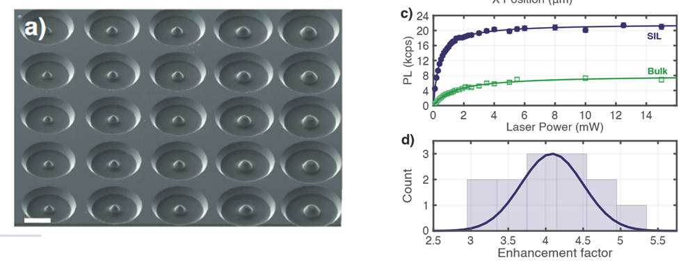
Below you can see an example of solid immersion lenses developed by a novel scalable gray-scale lithography process (App. Phys. Lett. 2023), with the corresponding enhancement in photon emission rate:
If you are interested in this topic, you can read our review on SiC photonics (2022), or a perspective we have co-authored with the QuanTELCO consortium about the role of SiC for future secure quantum networks. For more information on this work, please contact Prof Cristian Bonato or Dr Christiaan Bekker.